In the heart of California lies the world-renowned Silicon Valley, a technological hub that has shaped the future in ways unimaginable. But behind the scenes, away from the glitz and glamour of tech giants, there exists an unsung hero -. This critical process plays a pivotal role in ensuring the quality and performance of microchips, which power everything from our smartphones to spacecraft. We’ll delve deep into the world of Wafer Inspection in California, exploring its significance, challenges, and the cutting-edge technologies driving this essential facet of the semiconductor industry.
The Foundation of Silicon Valley:
- The Birth of Silicon Valley
Silicon Valley’s roots date back to the early 20th century when Stanford University faculty and graduates started setting up innovative companies in the region. What began as a center for radio and military technology during World War II gradually transformed into the global tech mecca we know today.
- The Semiconductor Revolution
The real turning point for Silicon Valley was the emergence of the semiconductor industry in the 1950s. Companies like Fairchild Semiconductor and Intel laid the foundation for the region’s dominance in the world of electronics. This industry’s growth paved the way for the development of cutting-edge technologies, including wafers and inspection.
What Are Semiconductor Wafers?
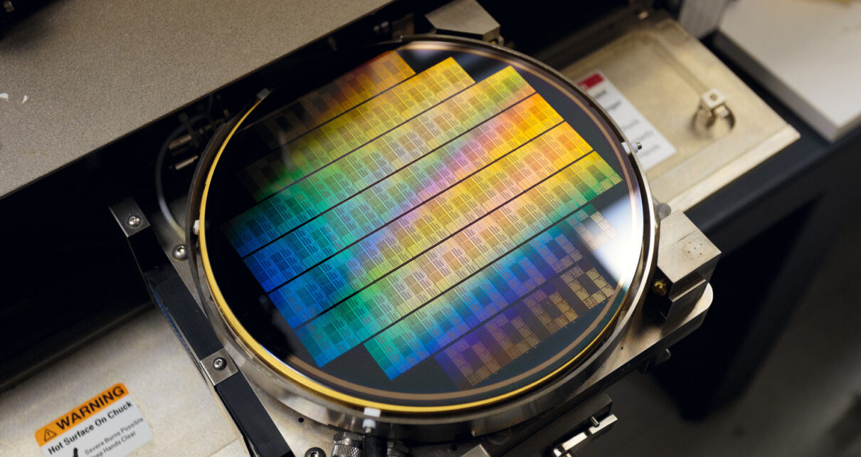
At the heart of every microchip is a semiconductor wafer, typically made of silicon. These wafers serve as the canvas for intricate circuits that form the basis of modern electronics. The quality of these wafers directly impacts the performance and reliability of electronic devices.
Creating semiconductor wafers is a highly precise and intricate process. It involves growing a single crystal of silicon, slicing it into thin wafers, and then meticulously adding various layers and patterns of materials using advanced fabrication techniques. Throughout this process, wafer inspection plays a crucial role in ensuring that each wafer meets the strict quality standards.
What Is Wafer Inspection?
Wafer inspection is a quality control process that involves scrutinizing semiconductor wafers at various stages of production. Its primary goal is to identify defects, irregularities, or impurities that could affect the functionality of the final microchip.
The Importance of Defect Detection:
Detecting defects early in the manufacturing process is paramount. A single microscopic flaw can render an entire wafer, and by extension, a batch of microchips, useless. This makes wafer inspection a critical step in ensuring the reliability and efficiency of electronic devices.
The Evolution of Wafer Inspection Technology:
- Early Days Visual Inspection
In the early days of semiconductor manufacturing, wafers, and inspection was a manual process. Skilled technicians would visually inspect wafers under microscopes, painstakingly identifying defects. This method was slow, labor-intensive, and prone to human error.
- The Rise of Automated Inspection
The need for greater accuracy and efficiency led to the development of automated wafers and inspection systems. These systems utilize advanced imaging techniques, such as bright-field and dark-field microscopy, to examine wafers at a microscopic level. They can process thousands of wafers per hour, significantly increasing production throughput.
- The Role of Machine Learning
In recent years, machine learning and artificial intelligence have made their mark in wafers and inspection. These technologies can analyze vast amounts of data to identify even subtle defects that might escape human observation. Machine learning algorithms continually improve their accuracy, making them invaluable in the quest for flawless wafers.
Challenges in Wafer Inspection:
- Shrinking Feature Sizes
As semiconductor technology advances, the size of circuit features on wafers continues to shrink. This miniaturization presents a significant challenge for wafers and inspection systems, as defects become harder to detect.
- Complex 3D Structures
Modern microchips are not flat; they often have complex 3D structures. Wafer inspection systems must adapt to these intricacies, ensuring that defects hidden within these structures are detected.
- Data Overload
The high-resolution images generated by wafer inspection systems result in massive amounts of data. Processing and analyzing this data in real time require advanced computing power and algorithms, posing a computational challenge.
Wafer Inspection in California:
- The Californian Semiconductor Industry
California, particularly Silicon Valley, is home to some of the world’s leading semiconductor manufacturers. These companies rely on state-of-the-art wafers and inspection technology to maintain their competitive edge in the global market.
- Research and Innovation Hubs
California boasts numerous research and innovation hubs dedicated to semiconductor technology. These institutions collaborate with industry leaders to develop and refine wafer inspection techniques, driving progress in the field.
The Future of Wafer Inspection:
- Nanoscale Inspection
The future of wafer inspection lies in nanoscale inspection techniques. As semiconductor features continue to shrink, new technologies are being developed to inspect wafers at the atomic level, ensuring even greater precision.
- Quantum Computing and AI Integration
The integration of quantum computing and advanced AI algorithms is expected to revolutionize wafer inspection. These technologies will not only enhance defect detection but also optimize manufacturing processes.
- Sustainability and Environmental Impact
As the semiconductor industry grows, so does its environmental footprint. Future wafer inspection methods will likely focus on minimizing waste and energy consumption while maintaining high-quality standards.
Conclusion:
In the sprawling landscape of Silicon Valley’s technological marvels, wafer inspection quietly plays the role of an unsung hero. It ensures the quality and reliability of the microchips that power our digital world. As we look to the future, the evolution of Wafer Inspection technologies in California and beyond promises to keep pace with the ever-advancing semiconductor industry, driving innovation and enabling the gadgets and technologies we rely on every day.